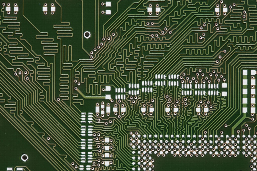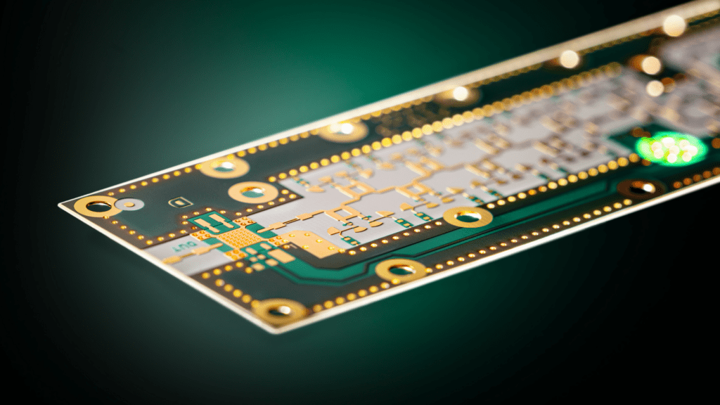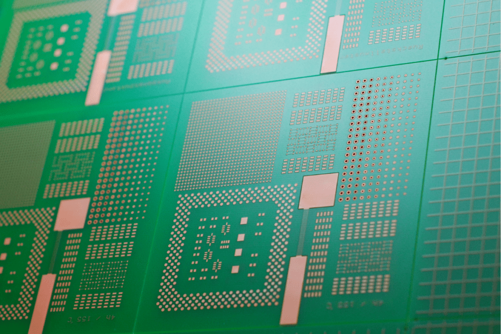
Soldering surfaces for printed circuit boards, Part 5: Organic Solderability Preservative (OSP)
Organic surface protection (OSP, or organic solderability preservative) is a cost-effective alternative to metallic surface finishes for printed circuit boards. An organic layer is formed on the exposed copper areas, which protects against oxidation by oxygen. This maintains the solderability of the PCB for a defined period of time without the need for an additional […]