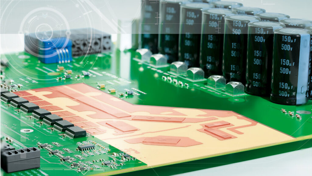
Iceberg® circuit boards
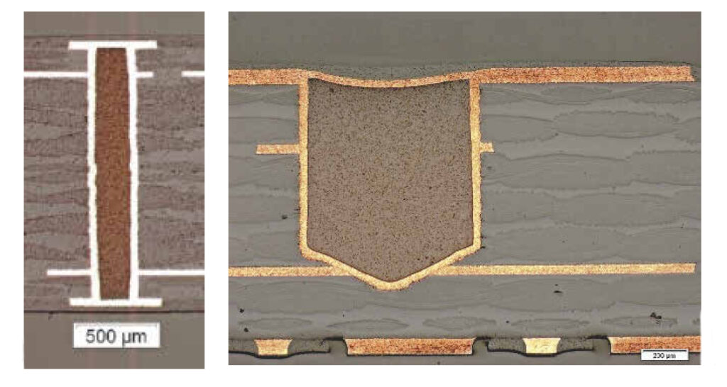
Iceberg® printed circuit boards are partial thick copper printed circuit boards with mixed copper thicknesses of 105 and 400 µm on the same plane in the outer layers. In the process, about two thirds of the thick copper is sunk into the base material. The “sinking” of the thick copper structures in the base material […]
Iceberg® circuit boards Mehr erfahren »