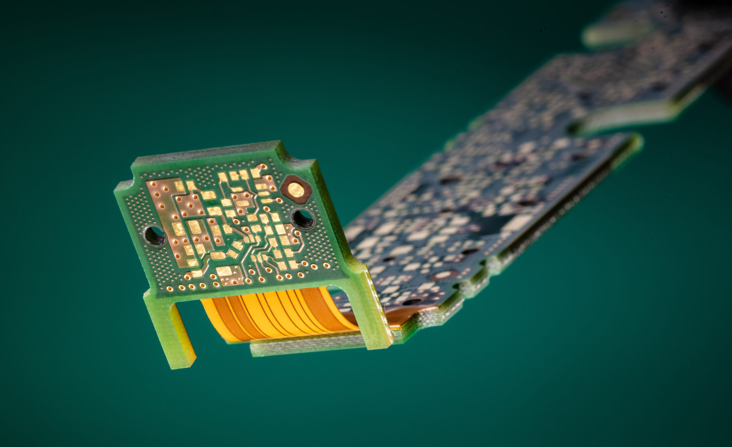
How to reduce costs in the production of rigid-flex printed circuit boards
Whether energy, raw materials or personnel – there is hardly any area that is not currently affected by exorbitant cost increases. This also has an impact on the production of printed circuit boards. This makes the question of potential savings all the more important, especially with complex components such as rigid-flex printed circuit boards. Several levers can be identified here that can contribute to greater cost efficiency.
Selecting the right base material
The base material is an important factor that can be influenced. It accounts for around 25-35% of the manufacturing costs and is a major factor influencing the process safety and reliability of the PCB. Therefore, the base material should always be selected according to the operating conditions and thermomechanical load. The question “What is really necessary?” plays a central role here.
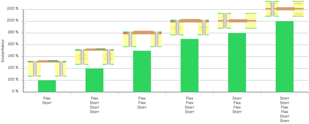
Cost comparison of different body variants
Concept of the layer structure
With rigid-flex PCBs, the right choice of layer structure is also cost-relevant. Considerable cost differences must be taken into account between layer structures such as “Asymmetrical one flex layer”, “Asymmetrical two flex layers” or “Symmetrical two flex layers”. At peak times, this can result in additional costs of up to 200%. In the Digital Design Compass you will find, among other things, the appropriate technical design-to-cost recommendations.
The right number of layers
Cost-oriented architecture is also based on the number of layers. This not only saves material, but also an entire inner layer production run per laminate, which corresponds to six to twelve work steps. If it is possible to reduce the multilayer structure by just one laminate, cost optimizations in the double-digit percentage range are often possible, depending on the complexity.
Avoidance of multiple grouting
The pressing process is also a significant cost driver. Multiple pressings mean multiple passes through an entire process chain and should therefore be avoided if at all possible. In this respect, it is advisable to avoid buried vias and to implement all connections from the outer layers wherever possible. In this way, one grouting and one drilling operation can be saved.
Optimum material utilization
One aspect that has a direct impact on all process costs is material utilization. If you want to operate efficiently here, you must therefore ensure optimum material utilization. This means that tolerances should only be as tight as absolutely necessary and that the focus should be on individual specifications or minimal restrictions for benefit design. Close coordination with the manufacturer is recommended here with regard to the cutting and PCB/panel sizes to be used, as offered by the KSG Group as part of its technical support.
Standardization instead of individualization
Even though there are no limits to individuality in the design of printed circuit boards nowadays, this is considered a cost driver. In order to be able to act as cost-efficiently as possible – especially with regard to quantity-dependent material purchase prices – standardization is required. Where technically possible, a dual-ply structure, standard laminate thicknesses and base copper thicknesses of 18 µm or 35 µm should be used. The use of adhesive rather than nonadhesive materials also makes a significant cost difference.
Just like customization, miniaturization also costs money and drives up material prices in particular, which is why the line space requirements should be as large as possible. This means that the manufacturer can work with standard copper thicknesses and does not have to resort to carrier-based copper foils in thicknesses of 9 µm or 5 µm, which have a material price that is up to 12 times higher.
Further XPERTS recommendations for rigid-flex PCBs:
- Involve the supplier in the development process as early as possible.
- Only restrict tolerance windows where absolutely necessary.
- Leave the delivery panel design to the supplier so that the circuit can be optimally aligned to the respective production panels.
- Specify the product so that the manufacturer can use flex lacquer instead of coverlay film for exposed, flexible areas. The application process is more cost-efficient due to the high degree of automation.
- If possible, switch to semi-flexible PCBs so that cost-intensive polyimide material can be dispensed with. In addition, the effort required for mechanical processing is reduced and lower drilling, milling, cleaning and metallization costs are incurred.