In an increasingly digitalized and fast-moving world, speed is of the essence. This applies to both everyday and industrial applications, be it wireless transmission systems, sensors or even radar applications.
An important building block for these high-frequency applications are high-quality and reliable printed circuit boards. But what exactly are the success factors for high-frequency PCBs and what do you have to pay attention to when planning and producing them? Experts from KSG Group provide answers to these questions.
Mr. Hackl, what is meant by high frequency and what role does the printed circuit board play in this?
The boundary between low and high frequency is assumed to be 10 MHz, since the typical thermal effects of high-frequency fields start to appear from here on. In the electromagnetic spectrum, the high-frequency range extends up to approximately 300 GHz. The typical high frequency range on the PCB is between 10 and 100 GHz.
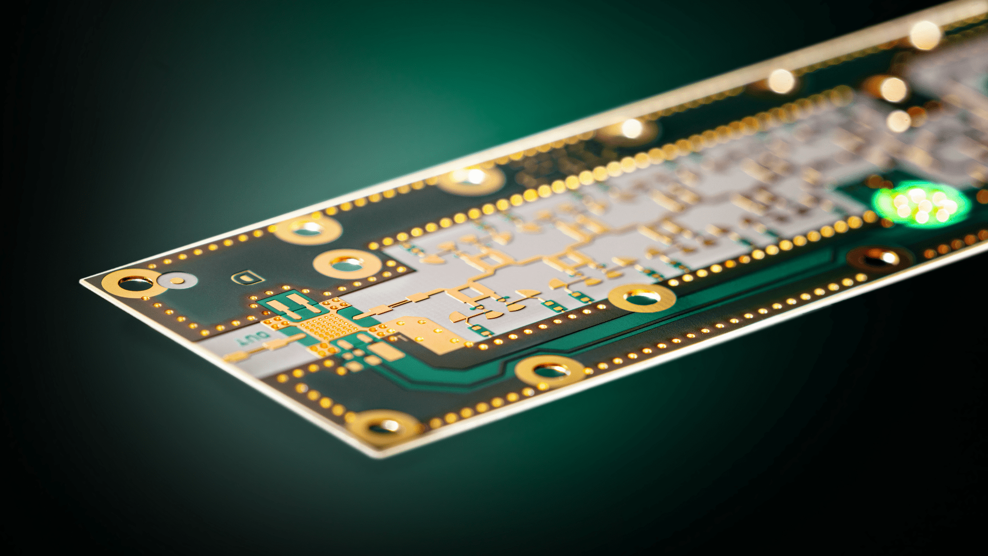
Here, the circuit board acts as a transmission element with deliberately trimmed conductor tracks for the transmission of high-frequency signals. The desired impedance of such lines is mainly dependent on the trace width and the defined distances to the plane reference layers. Etched high-frequency components on the PCB include, for example, finger couplers, filters, l/4 elements, patch antennas or ring resonators.

Interview: Johann Hackl
Johann Hackl from KSG’s Technical Support supports companies from the first minute of the product idea in an efficient and economical development of printed circuit boards suitable for series production. The expert knows what matters in high-frequency applications and discusses five important aspects of RF printed circuit boards below.
What are the basic requirements that an RF printed circuit board must meet?
In high-frequency applications, smooth and precise signal transmission is the be-all and end-all. Any irritation on the PCB leads to a reflection or change in the high-frequency signal, which is why a straight contour of the conductor routing is particularly important here. To illustrate this, I like to use the image of a rock in the surf, which we usually perceive as positive. But for high-frequency applications we do not want to have such a rock in the conductor path, at which the waves break. This means that irritations, indentations or impressions must be avoided.
In addition, since high-frequency signals are pressed against the outer skin according to the skin effect, all four sides of a conductor should be as smooth as possible. The critical side is the underside of the copper foil, which is artificially pretreated by oxidation. There are different roughnesses here, which should be as low as possible for high-frequency applications. At the same time, however, the minimum adhesive strength must also be satisfied.
What role does material selection play in high-frequency printed circuit boards?
Selecting the right material is an important success factor for RF printed circuit boards. The most important parameters for material selection include:
- the dielectric constant (Dk),
- the dissipation factor (Df),
- the stability of the RF characteristics over the relevant temperature range,
- the reliability after temperature-humidity stress,
- the copper adhesion strength,
- the dimensional stability,
- the water absorption,
- and the costs.
Especially the last point should not be underestimated, because the cost of high-quality high-frequency materials is enormous. Therefore, it is recommended to contact experienced project engineers at an early stage to find the most suitable and at the same time the minimum necessary material in terms of cost.
What must be taken into account when processing the materials?
Drilling and also milling of PTFE materials are further success factors for HF printed circuit boards. It is essential to optimize the respective drilling or milling parameters depending on the material used. For drilling, these would include the tool type, cutting speed, feed rate and return stroke. Mixed structures are often used for cost reasons, and their properties must be taken into account in any case in order to find the right parameters and tools. After all, in addition to low tool wear, we naturally want to achieve good cutting quality here, and without fringes and smearing.
What is important in the conductor pattern structuring of RF layouts?
When implementing HF layouts within narrow tolerance limits it may well be necessary for individual ladder elements in the film templates to be need to be adjusted. Particular attention should be paid to the following Aspects:
- Minimization of corner rounding of individual
- Layout element
- Compliance with the required edge steepness
- Avoidance of excessive edge roughness due to
- Remaining treatment peaks
Structural fidelity can be checked by means of an automatic optical inspection of relevant RF layers, at best during the first production panel. Here, the individual layout elements are measured and critical elements are displayed so that the rest of the batch can be etched with the same parameters or with adjusted parameters if required.
Tilo Leistner will give a more detailed insight into the etching process and the final inspection in the upcoming videos:
Even more RF PCB knowledge
A comprehensive and intensive insight into the world of high-frequency printed circuit boards was provided by Johann Hackl and Tilo Leistner at the XPERTS webinar “Need for Speed” given in October 2022. The recording of the webinar is available on-demand -. register now.