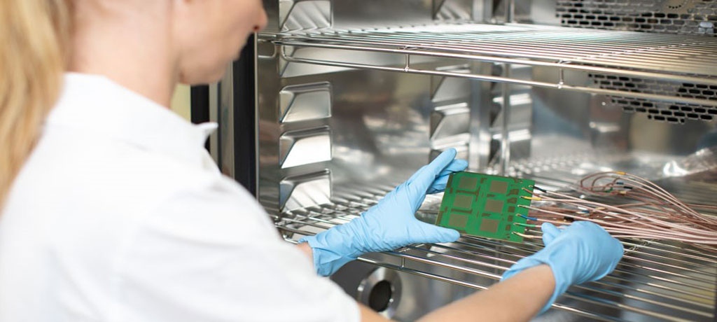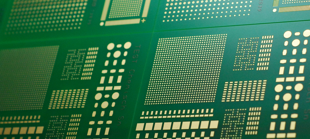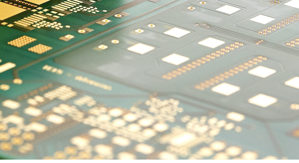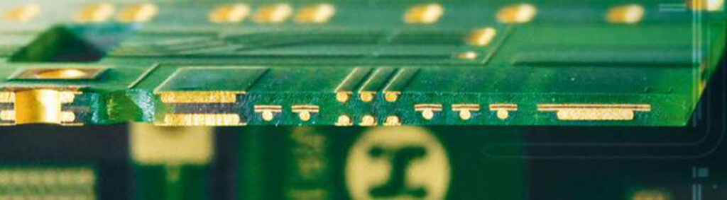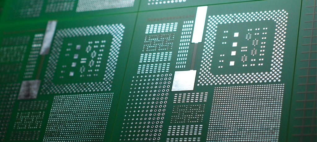
Solder Surfaces for Printed Circuit Boards, Part 4: HAL lead-free
The HAL lead-free solder surface offers the best solderability of all surfaces, but the thickness of the tin layer varies.
Solder Surfaces for Printed Circuit Boards, Part 4: HAL lead-free Mehr erfahren »