The most important questions and answers
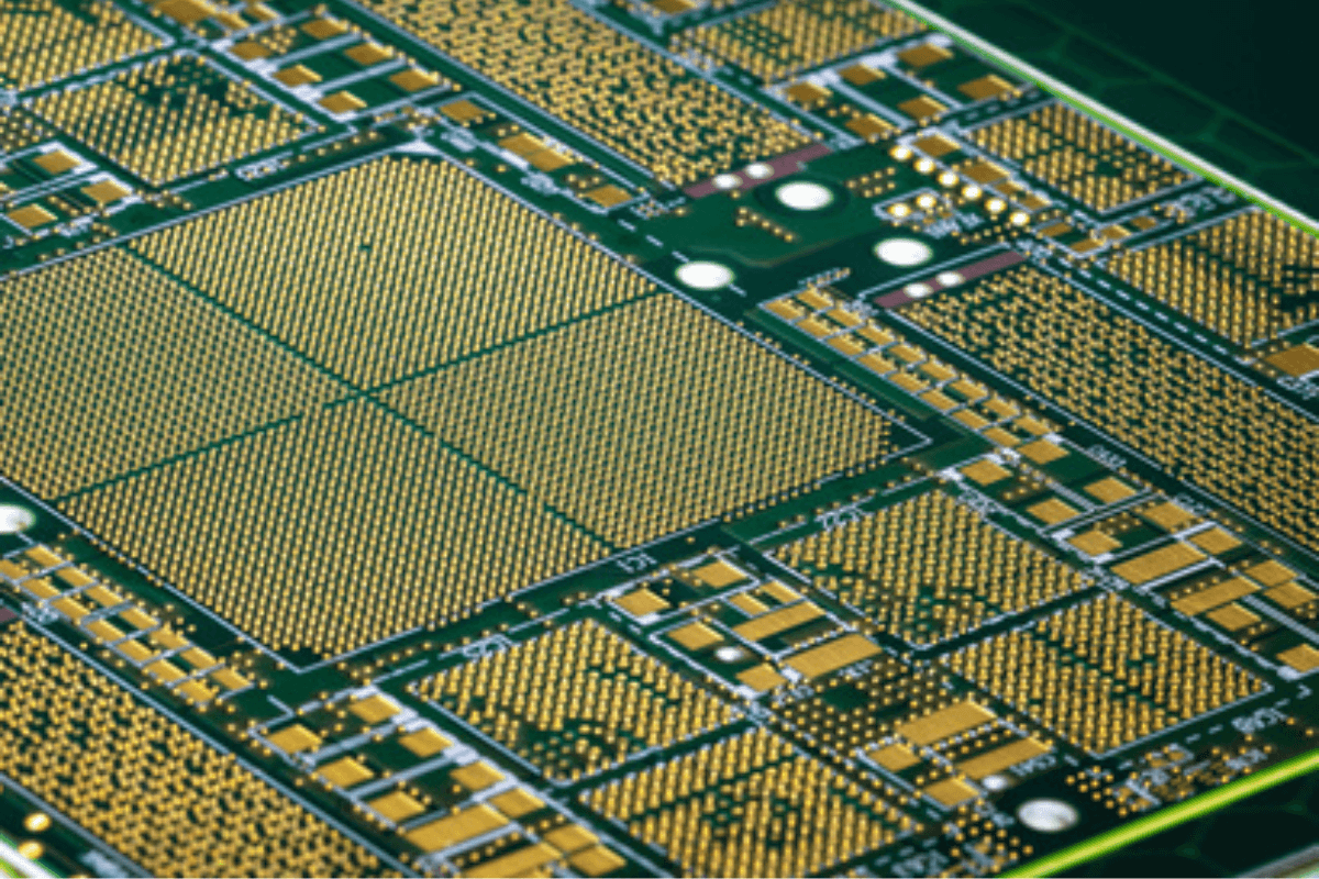
They are used in smartphones, aircraft and medical equipment and enable high technical performance in the smallest of spaces: HDI printed circuit boards have become indispensable in the electronics industry. However, with advancing miniaturization and, at the same time, increasingly complex circuits, the demands on the design and manufacture of multilayer printed circuit boards are rising.
What characterizes an HDI printed circuit board?
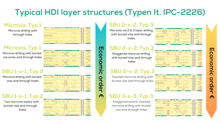
HDI printed circuit boards are compact multilayer printed circuit boards with four or more layers, which are usually built up sequentially in several press cycles using SBU (Sequential Build Up) technology. HDI stands for High Density Interconnect and means high circuit density. This can be achieved by a multilayer structure of the PCB, line structures and spacings of < 150 µm and vias with a size of < 150 µm (often MicroVias).
Technology & design to cost at a glance
Whatrequirements are placed on PCB manufacturers?
On the one hand, PCB manufacturers must pay attention to the suitability of the base materials. The most important factors here are the lowest possible laminate and copper thicknesses and a low coefficient of thermal expansion. On the other hand, ever smaller line space structures go hand in hand with higher demands on plant technology. DI (direct imaging) imaging is gaining importance here, offering not only high layout resolution but also better positioning accuracy. DI exposure is also gaining ground in the solder resist sector. Direct exposure of the resist can reduce the stop varnish web and reduce stop varnish exposure by pads. High demands are also placed on the etching process in the HDI area, where a uniform top and bottom etch rate must be ensured.
What should be considered in the PCB layout of HDI printed circuit boards?
As a general rule, it is advisable to contact the PCB manufacturer as early as possible in order to know their options. Finally, at the end of the layout process, there should be a layout that is ready for the manufacturer. On the developer and layouter side, the first thing to do is to describe what the future PCB should look like. Among other things, the following questions must be answered:
– Which base material should be used?
– How many layers are needed?
– Where are holes in the stack?
– Which base copper thicknesses are required?
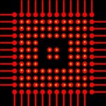
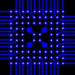
– Are components with high connection density (e.g. BGA) used?
This often results in the routing strategy for the entire layout, and the layer structure and constraints can be defined for all parameters, e.g. conductor track widths, distances and sizes for blind and buried vias.
Example: BGA unbundling

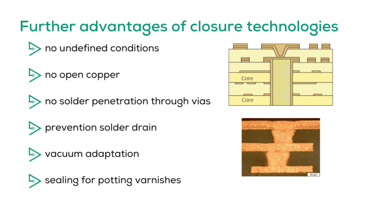
What role do closure technologies play in HDI printed circuit boards?
Although they involve higher process costs, closure technologies such as microvia copper filling or plugging according to IPC-4761 Type VII a number of advantages. These include, in particular, extended design and unbundling options as well as space savings due to an almost planar surface topography. In addition, air and media inclusions can be prevented and assemblies can be protected with potting varnish. In addition, if microvias are also used for heat dissipation, the thermal performance of HDI circuit boards can be enhanced.
Where is HDI headed - what else is possible in the future?
In the medium and long term, it will be possible to use even thinner materials with better properties and to increase the number of pressing operations. There will also be further advances in miniaturization, so that even smaller structures can be realized both in the conductor pattern and in the stop varnish, and even smaller holes can be processed reliably.
Do you have further questions?
You can find even more information about HDI printed circuit boards in our XPERTS online seminar “HDI – Geht’s noch : Möglichkeiten zur Entflechtung hochintegrierter Bauelemente” with Thomas Doberitzsch and Dirk Deiters. You can register for the on-demand version available at any time register here.