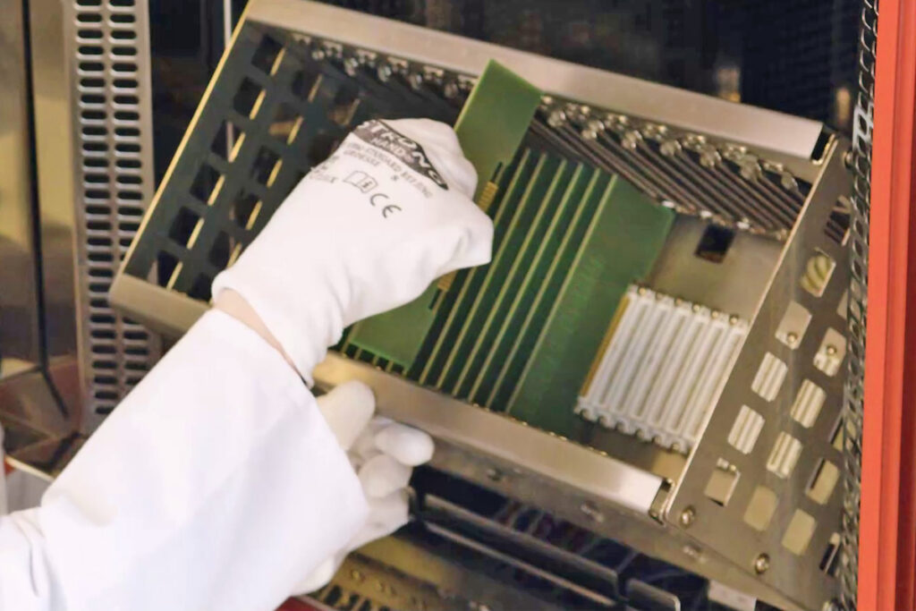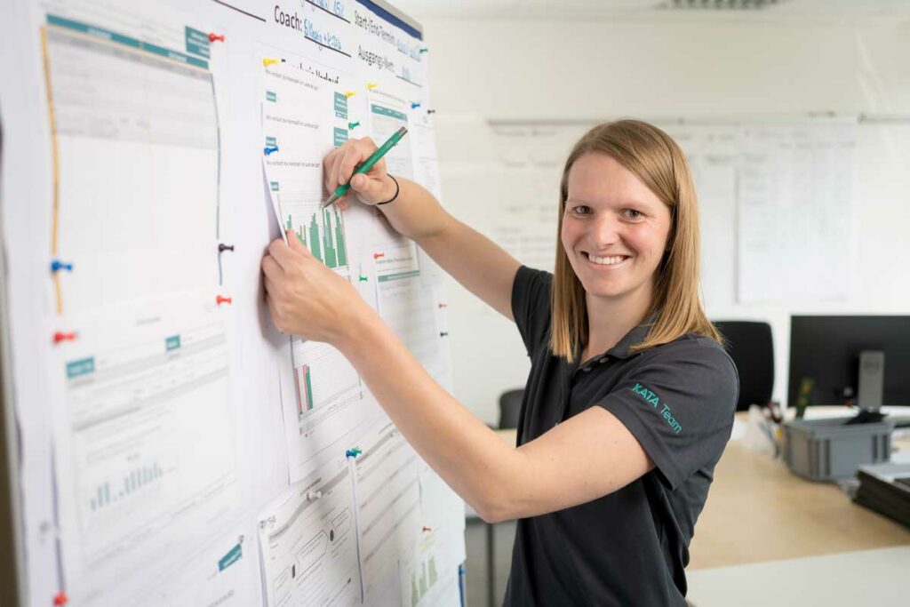
How does lean management work at one of Germany’s leading printed circuit board manufacturers?
From process optimization to digitalization: KSG provides insight into practice.
From process optimization to digitalization: KSG provides insight into practice.
To ensure that printed circuit boards work reliably even under high temperature fluctuations, they are intensively tested in advance. KSG explains how.
5+1 questions about the temperature change test Mehr erfahren »
Today is World Bee Day, for us from KSG a reason to celebrate our little black and yellow employees.
World Bee Day – A great day for our smallest workers Mehr erfahren »
In Germany, industry accounts for around 31 percent of annual energy consumption. If the energy revolution is to succeed, companies must accept their responsibilities by reviewing and auditing consumption and looking for ways to optimize it. With rising energy prices, this makes sense not only ecologically, but also economically. In addition to consumption, there is
The printed circuit board manufacturer KSG has mastered the past 18 months with entrepreneurial skill and customer service. The business situation is pleasing and the team has grown to meet the challenges. “We learned three things in the Corona crisis,” says CEO Margret Gleiniger. “Firstly, that we can change ad hoc and that changes are
The stress test showed how agile and mobile our company is Mehr erfahren »
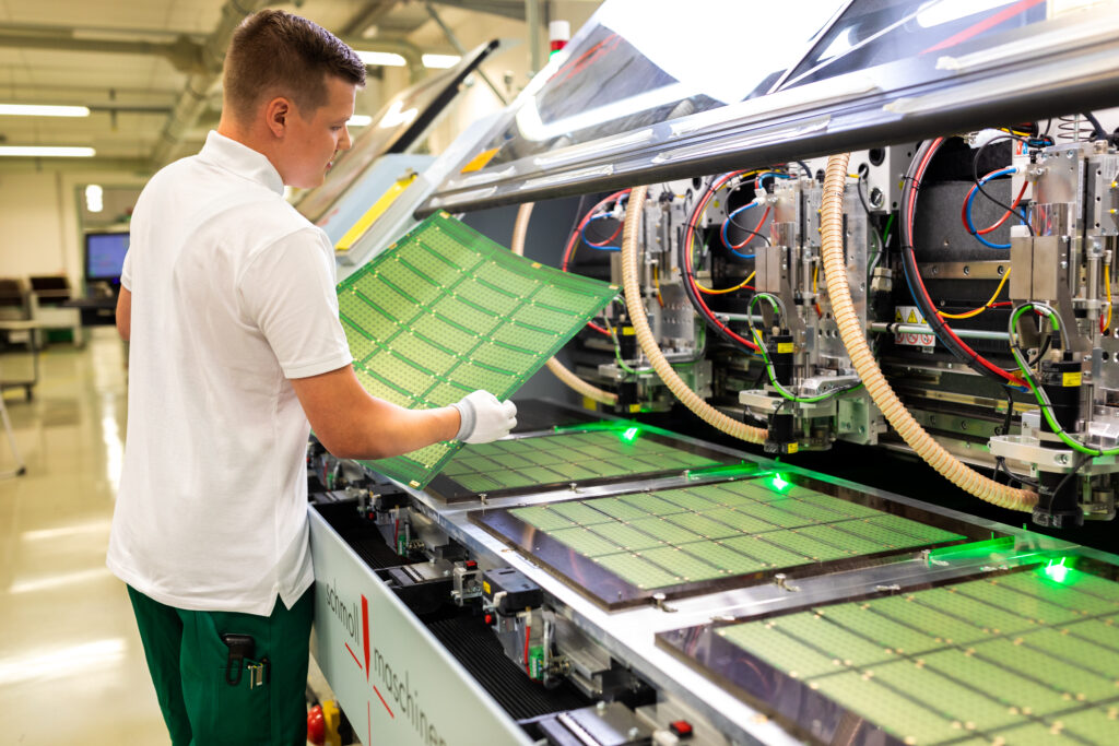
ENAL = Use of nano-coated tools in printed circuit board production Approximately ten percent of the manufacturing costs of a printed circuit board are caused by the mechanical manufacturing processes, drilling and milling. The costs for drilling and milling tools play a not insignificant role. Together with KSG, a Saxon project consortium within the framework
Short portrait of the ENAL funding project Mehr erfahren »
Design rules for high current conductor paths These rules must be observed when designing HSMtec printed circuit boards: Standard values for HSMtec PCBs are 0.8 to 3.2 mm final thickness; maximum 12 layers; maximum 3 layers for the copper cross-sections with copper profiles as well as currents up to 400 A Basic rule for current
Tips for PCB design with copper elements (HSMtec) – Part 2 Mehr erfahren »
When designing HSMtec-PCBs with integrated copper elements, it is generally recommended to design the high-current conductors before the standard layout. The development process of an HSMtec printed circuit board takes place in 10 design steps: Define mechanical features: Determine the size and contour of the printed circuit board Place power components: define short and simple
Tips for PCB design with copper elements (HSMtec) – Part 1 Mehr erfahren »
Interview with Margret Gleiniger (CEO/CFO) and Swen Klöden (CTO) of KSG GmbH and Kornel Schmidt, Managing Director of KSG Austria GmbH Made in Europe’ is anything but a matter of course when it comes to the manufacture of printed circuit boards. KSG GmbH manufactures a wide range of printed circuit boards for the international market
Printed circuit boards with flexibility (Business Forum, August 2021) Mehr erfahren »