Design rules for high current conductor paths
These rules must be observed when designing HSMtec printed circuit boards:
Standard values for HSMtec PCBs are 0.8 to 3.2 mm final thickness; maximum 12 layers; maximum 3 layers for the copper cross-sections with copper profiles as well as currents up to 400 A
Basic rule for current carrying capacity: For each copper profile of its width, the conductor track must be designed 1 mm wider all around. Example: An 8 mm copper profile requires a 10 mm wide conductor track.
The copper profiles must not be placed on adjacent layers.
A potential-independent copper support of at least the same size must be provided on the opposite FR4 core side of the copper element. This copper layout is potential-independent and serves to clearly support the copper profile for ultrasonic welding.
For economic reasons, it is important to route the high-current conductor paths directly and in a straight line (with as few changes in direction of the high-current connections as possible). Branches in the copper profiles can be realized via etched surfaces.
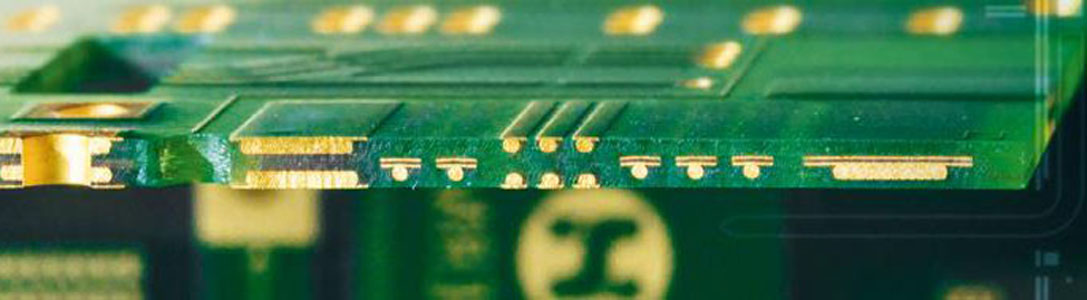
Copper profiles are available in four widths: 2, 4, 8 and 12 mm with a variable length, but it should not be less than 15 mm.
The distance between the profiles should be at least 2.20 mm.
Layer changes of copper profiles from inner layers to outer layers (and back again) are possible without any problems with through-platings.
The high-current printed circuit boards are suitable for all common connection contacts: screw, pressure contact, press-fit or soldering.
Microvias and Thermovias can be used to thermally connect the copper profiles to a heat sink. Conductor widths, residual rings and aspect ratios must be observed so that a sufficiently large amount of copper is deposited. A minimum copper thickness of 20 µm must be achieved in the bore.
Since the power components become hotter than the high-current conductor, a thermally optimized design is required.