English
Tips for PCB design with copper elements (HSMtec) – Part 2
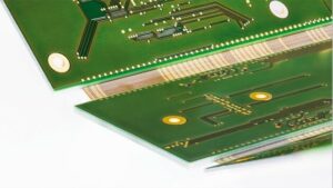
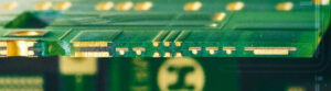
Design rules for high current conductor paths These rules must be observed when designing HSMtec printed circuit boards: Standard values for HSMtec PCBs are 0.8 to 3.2 mm final thickness; maximum 12 layers; maximum 3 layers for the copper cross-sections with copper profiles as well