Incorrect handling and improper storage of printed circuit boards have fatal consequences. Contamination, moisture and electrostatic charge can irreparably damage printed circuit boards or later electronic assemblies, reduce solderability and affect the electrical test.
Absorbed moisture in base materials can cause internal delamination, twisting and warping, or excessive stresses in the through-metallizations. The reason: During soldering, the absorbed moisture evaporates explosively and delamination or other damage to the PCB is caused. Therefore, the printed circuit boards should be stored either vacuumed and packed airtight or dry in shrink film in accordance with ESD requirements (see following storage conditions).
The professional storage of printed circuit boards is described in the IPC-1601 guideline. There is also a ZVEI recommendation for implementation.
We have summarized the most important rules for proper storage to prevent PCBs from absorbing moisture and to maintain optimal solderability:
- Leave the printed circuit boards in the closed transport packaging until assembly.
- store under the storage conditions specified below
- Observe solderability period (see below)
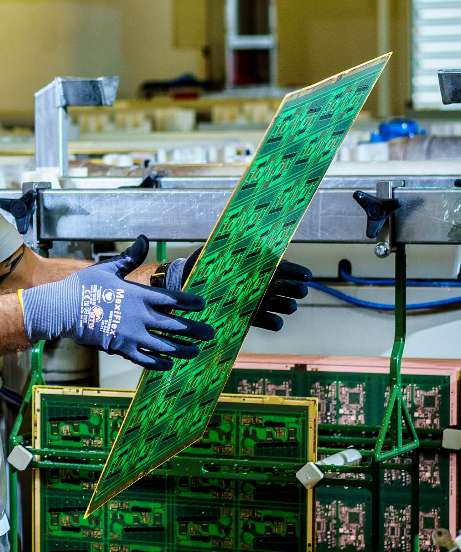
- Touch the edge of printed circuit boards with clean gloves
- Do not touch soldering surfaces directly with the hands
- Process printed circuit boards from opened transport packaging after a maximum of one week
Storage Conditions:
- Storage temperature 20 °C ± 5 K
- Relative humidity: max. 60 %
- Avoid direct sunlight
Storage periods of the printed circuit board surfaces (under the above storage conditions):
- Electroless nickel/gold: 12 months
- Chemical tin: 9 months
- HAL lead-free: 12 months
- Entek Plus: 6 months