Semiflex printed circuit board: the low-cost alternative to rigid-flex
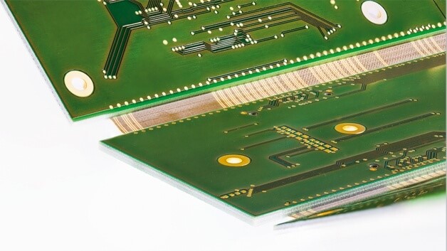
Semiflex is considered a cost-effective alternative to rigid-flex technology. The absence of flex foils lowers the price, but also reduces the bending properties. The moving areas are created here by deep milling in the FR4 circuit board, and the residual thickness is only approx. 150 µm. The printed circuit board can therefore be bent in this area together with the conductor tracks placed on it and the flex coating or cover film applied over the conductor tracks. In contrast to the rigid-flex technique, the bending radius must be at least 5 mm. The Semiflex structure is well suited for static bending stress during assembly and installation. In the simplest case, a part of the PCB can be bent after assembly and fixed in this position during installation in the control cabinet.
One example of this technology is the newly developed test bench from the company LSP Innovative Automotive Systems for the automotive sector. This test bench is used for the electromotive control of the 16 gas exchange valves of a research combustion engine. For assembly and space reasons, the control unit of four valves of a cylinder is combined into a U-shaped module. Test bench measurement signals are acquired in the middle part of the board and must be distributed to the side wings. Since a solution with connectors was too large for the available installation space, Semiflex technology was chosen as the most suitable and cost-effective PCB technology.
When flat, the Semiflex PCB measures 413 mm x 276 mm and consists of six layers of 70 µm copper each. The areas to be bent by 90° during assembly have a length of 8.5 mm and the total width of all bending areas is 426 mm. A total of 195 conductive tracks are laid over the four partially flexible areas. Bent twice by 90°, the PCB only requires a volume of 175 mm x 67 mm x 276 mm when assembled. Current routing to the power components and even heat dissipation could be realized with embedded copper profiles on the same PCB.
3D printed circuit boards: three technologies, three examples (part 1)