In “HAL lead-free” (hot air leveling lead-free), hot air solder leveling or HASL (hot air solder leveling), a layer of liquid tin is applied to the exposed copper surfaces. The circuit boards are first wetted with flux and then immersed in a vertical solder bath. When the PCBs are pulled out of the solder bath, excess solder is blown off with hot air. The printed circuit boards are then cooled in a horizontal process section.
What speaks for “HAL lead-free”?
“HAL lead-free” is the RoHS-compliant (2011/65/EU) further development of hot air tinning with tin/lead solder, which was already used in PCB production in the 1960s. For “HAL lead-free”, KSG uses a bar solder made of an alloy containing 99.7% tin and 0.3% silver with a melting point of 217 to 227 °C. The tin-plating temperature is specified as 270 °C in accordance with UL. From a soldering point of view, hot air tinning offers the best solderability among all surfaces. Tin and copper of the connecting surfaces form an intermetallic compound zone (IMC). If stored properly, the PCB manufacturer provides a 12-month warranty on solderability.
Short info “HAL lead-free
Alloy: 99.7% tin | 0.3% silver
Melting point: 217-227 °C
Tin plating temperature according to UL: 270 °C
Process-related irregular thickness of the tin layer
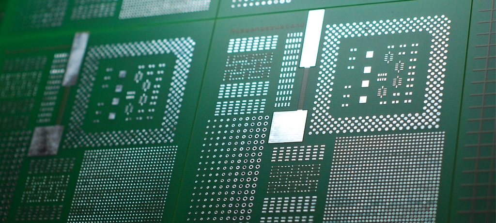
Hot air tinned solder connections are characterized by relatively large variations in the layer thickness or no planarity of the surface. The reason is the physically induced solder meniscus formation (see picture) due to the blowing off of the excess solder. Therefore, this surface is not suitable for fine-pitch SMT components.
Wetting of solder pads is evaluated in accordance with J-STD-003. The thickness of the tin layer is defined from “covered” with approx. 1 µm at the hole entrance for THT connections to ≤ 40 µm in the pad center. The coating thicknesses can be determined destructively by means of grinding. In the “HAL lead-free” process, the base material of the PCB is subjected to high thermal stress due to the large, relative temperature swing (from room temperature to 270 °C) of lead-free solder. Therefore, HAL lead-free is not recommended for standard Tg-FR4 base materials.
Further advantages of “HAL lead-free
HAL lead-free can be combined with electroplated nickel/gold for connector contacts. Hot air tinning is suitable for press-fit technology. The surface is unsuitable for any wire bonding processes. Compared to the insensitive ENIG and the sensitive chemical tin, HAL lead-free is in the middle. In concrete terms, this means that the surface is quite insensitive to thermal processes that follow the application of the soldering surface, e.g. the curing of lacquers or drying processes of the PCB before component assembly. In a direct comparison of process costs, lead-free hot air tinning is cheaper than electroless nickel/gold and electroless tin soldering. Hot air tinning has a share of approx. 20 % of all solder surfaces used in Europe; the trend is downward.
https://youtu.be/9IjKzUqWAow
Would you like to learn more about the processes, properties and advantages and disadvantages of the individual solder surfaces? Then take a look at our XPERTS online seminar. There, Annett Horbach and Matthias Stickel will give you numerous practical tips on choosing the right end surfaces for you. Sign up directly!
