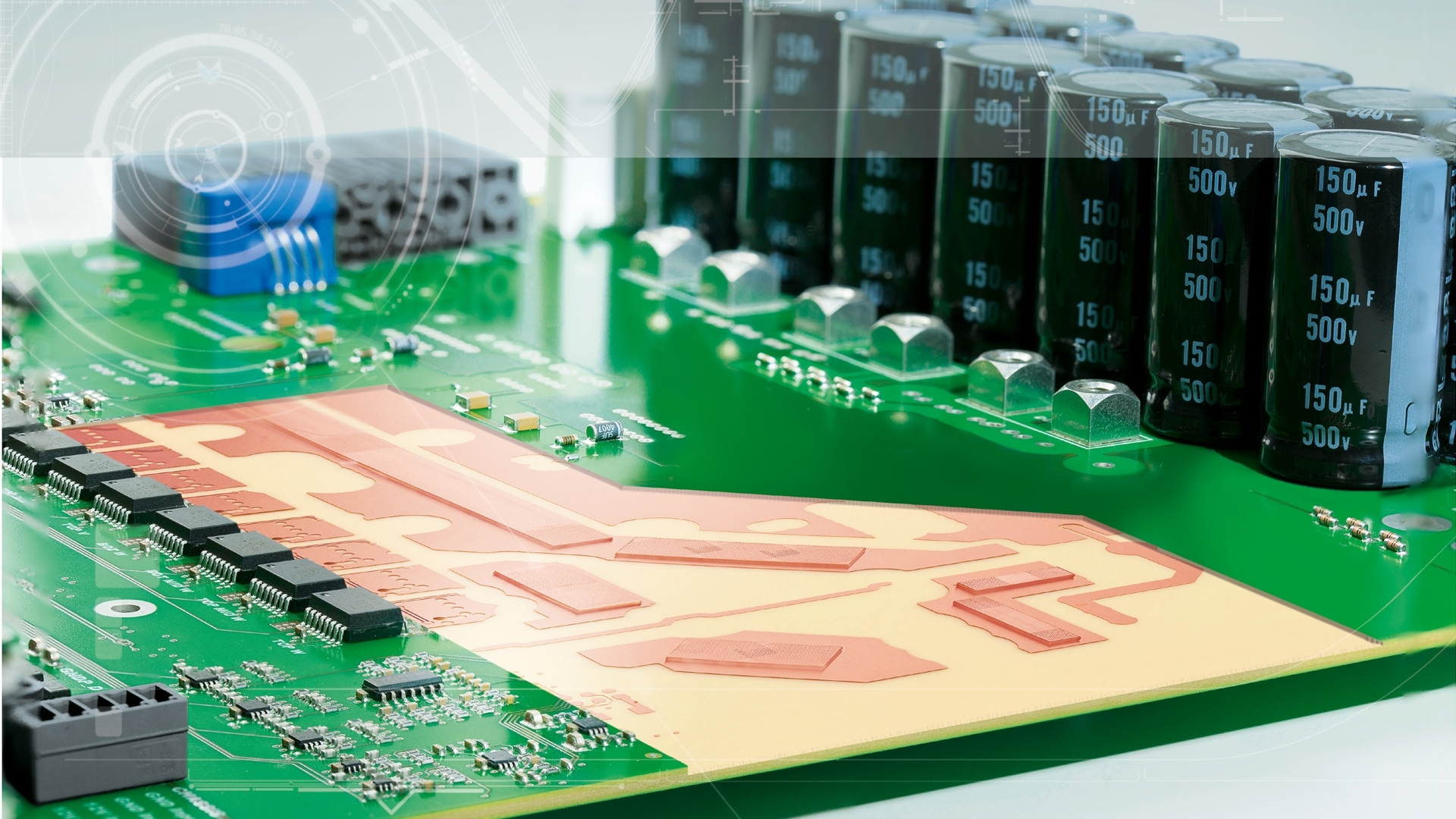
In the HSMtec process, 500 µm thick copper elements with variable widths from 2 to 12 mm and individual lengths are placed in the inner layers of the multilayer and embedded in the printed circuit board. By partially integrating copper profiles into the PCB, high-current paths – or thermal management and fine conductor layout – can be easily combined and adapted to the spatial conditions. Since the copper profiles are partially integrated into the PCB, load and logic or power and control electronics can be combined on one PCB.
The copper elements are bonded to the etched inner and/or outer layers using ultrasonic bonding technology. The integrated copper elements transmit currents of up to 400 A and also quickly reduce heat generation to permissible part and system temperatures. This allows easy integration into a standard multilayer manufacturing process with subsequent pressing of the individual layers. Thanks to a large number of design variants, high currents and power losses of components can be selectively fed into printed circuit boards – without any further external work steps.
