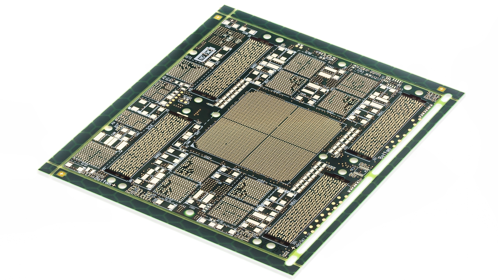
The abbreviation HDI stands for High Density Interconnect and refers to multilayer printed circuit boards with four or more layers that are built up sequentially in several pressing operations (Sequential Build Up, abbreviated: SBU). With this design, high wiring and placement densities for high-pole active components can be realized on an electronic assembly.
Typical of an HDI PCB is a high wiring density in conjunction with a very high number of microvia holes, or microvias for short. We speak of HDI with conductor structures from 150 µm and finer, and of microvias with a hole diameter <0.2 mm. Modern production technology enables layouts from a line/space of 75 µm. Hole filling technologies, e.g. microvia copper filling, plugging or resin filling, play a crucial role in choosing an optimal rewiring strategy.
The advantages are:
Maximum packing densities, miniaturization and best possible use of space,
Greatest possible freedom in the placement of components,
Shortening of the conductor lengths and improvement of the EMC behavior of the assembly,
Simplified unbundling of the PCB layout, reduction of the number of layers,
Dense, single-sided assembly and associated reduction of assembly costs